Main

XBox Remote Project Archives

June 16, 2007

Loomings

To work! Here are the bits and pieces I'll be playing with:

EZ430-F2013

ez430_f2013_top.jpg

ez430_f2013_bottom.jpg

(I'll call it the "f2013" from now on.) The f2013 has 14 through-holes in the tiny board which contains the microcontroller. These 14 pins connect directly to the 14 pins of the microcontroller. The f2013 as shipped is inside a plastic case; with a little care it's easy to pry apart the two halves of the case to get access to the f2013 board. Notice that I've soldered a 2x7 connector to the proto holes in the f2013.

Pins of the connector are labeled according to the micro pin they connect to, for example "P3" connects to microcontroller pin 3. The pins are physically arranged like this, if you're looking at the top view of the board (looking at the the connector pins as they are soldered into the through holes) with the USB connector on the left:

P14P1
P13P2
P12P3
P11P4
P10P5
P9P6
P8P7


1c20 board (links to pdf)

1c20_board.jpg

This is a development board for a perfectly decent, but rather old FPGA - the Cyclone 1c20. Since I work for Altera, it's easy for me to get my hands on one of these boards. I chose this board because it still works just fine with modern tools. Any dev board with a santa cruz connector would work equally well.

J15 is a handy 14-pin connector in a 2x7 arrangement, just right for plugging the f2013 into. Well. Almost just right. More below. Here's the pinout:

j15.GIF


If I blindly plugged the f2013 into J15, these are the connections that would result:

J15 pinJ15 functionf2013 pinf2013 function
J15-1GNDP14GND
J15-2+5VP1VCC
J15-3R11P13XIN
J15-4Y9P2P1.0
J15-5W9P12XOUT
J15-6T10P3P1.1
J15-7U10P11TEST
J15-8V10P4P1.2
J15-9W10P10RST
J15-10Y10P5P1.3
J15-11V11P9P1.7
J15-12U11P6P1.4
J15-13W11P8P1.6
J15-14Y11P7P1.5

The problem is on the second line of the table: J15-2 is +5V, but the f2013 VCC is only 3.6V. Bad things will happen if I connect those two power supplies! I could physically remove that pin of the 2x7 header soldered to the f2013, but in the ultimate application, that pin may be used for supplying power. Or, I could cut the +5V pin on J15, but I don't really want to modify the 1c20 board. Solution: don't plug the f2013 directly into the 1c20 board; instead, plug it in via an intermediate board, which will connect every pin except for J15-2/P1.

Santa Cruz Connector Prototype Board

sc_board.jpg

This is a handy little prototype board which plugs into the "santa cruz connector" footprint of the 1c20 board. I've carved away the connection of J15-2, so that the 1c20 board's +5 supply doesn't connect to the board. The f2013 board connects right into the santa cruz board:

on_sc_card.jpg

And then the santa cruz board plugs into the 1c20 board:
complete_system.jpg

That's enough for now - next time, I'll cover the process of building a testbench, a.k.a. a binary configuration file for the FPGA.

June 18, 2007

Wires Are Your Enemy

So, I've replaced a simple, cheap breadboard containing a few wires and an LED with an expensive, very complex circuit board containing, among other things, an FPGA which is much more sophisticated than the microcontroller I want to use. I'm depressed. What was the point, again?

To restore my optimism, I need to see some tangible results. I'll start with a nice simple application. The first testbench configuration for the FPGA will consist only of pins and wires; everything else in the FPGA will be left idle. Here's a block diagram of the system:

tb_1_system.gif


All of the microcontroller's pins (except VCC and GND) connect to the 1c20 board through J15, but in this design I'll only use 8 pins: P1.0 - P1.7. The FPGA will just be wires - it'll connect in0 to out0, in1 to out1, et al. The 8 outputs, out0 - out7, will drive the 8 individual LEDs on the 1c20 board. Then I'll write some code for the f2013 which will drive a recognizable pattern onto P1.0 - P1.7, which will make the 8 LEDs blink. Sounds easy! But... how do I configure the FPGA?

Install the Altera design software (Quartus)
A free version of Altera's main design tool, Quartus, is available. Go to http://www.altera.com and look for the "Quartus Web Edition Software". I hope the installation procedure is self-explanatory. If you run into trouble, let me know.

Create and configure a quartus project
This can be done via the GUI, but I think I'll play with the scripting flow. This is based on tcl, which seems to be the lingua franca of the EDA world. Altera provides a command-line tool which executes tcl files, and a set of commands which manage projects, set design properties, etc. I'll only scratch the surface here. Let's get started! I created a tcl script, call it tb_1.tcl:

# Step 1: Create a new project called tb_1
project_new tb_1
project_open tb_1

# Step 2: Project settings:
# a. Choose the type of FPGA
set_global_assignment -name FAMILY Cyclone
set_global_assignment -name DEVICE EP1C20F400C7
# b. Any pins which aren't otherwise defined should be inputs.
set_global_assignment -name RESERVE_ALL_UNUSED_PINS "AS INPUT TRI-STATED"
# c. Declare the top-level file (well, the only file):
set_global_assignment -name VERILOG_FILE top.v
set_global_assignment -name TOP_LEVEL_ENTITY top

# Step 3: Set pin assignments. This is where the top-level ports of the testbench
# design are mapped to actual physical FPGA pins.

set_location_assignment PIN_Y9 -to in[0]
set_location_assignment PIN_T10 -to in[1]
set_location_assignment PIN_V10 -to in[2]
set_location_assignment PIN_Y10 -to in[3]
set_location_assignment PIN_U11 -to in[4]
set_location_assignment PIN_Y11 -to in[5]
set_location_assignment PIN_W11 -to in[6]
set_location_assignment PIN_V11 -to in[7]
set_location_assignment PIN_E14 -to out[0]
set_location_assignment PIN_E13 -to out[1]
set_location_assignment PIN_C14 -to out[2]
set_location_assignment PIN_D14 -to out[3]
set_location_assignment PIN_E12 -to out[4]
set_location_assignment PIN_F12 -to out[5]
set_location_assignment PIN_B3 -to out[6]
set_location_assignment PIN_B14 -to out[7]

# Step 4. That's all!
project_close

To execute this tcl script, I go to an empty directory, open a bash shell (use Quartus' version, in <quartus>/bin/cygwin/bin/, if you don't already have one handy), and run

quartus_sh -t tb_1.tcl

Now the directory contains a few new things: files tb_1.qsf and tb_1.qpf, and a db directory. The qsf file seems to be nearly a copy of tb_1.tcl, with some extra stuff added. Comments in the qsf file advise me not to modify the file. Well, ok.

Specify the design's logic
In tb_1.tcl, I declared that the project's top-level entity would be "top", and that there would be a verilog file called "top.v". To deliver on my promise, I must create a verilog file called "top.v" which defines a module "top" containing all the ports that I made pin assignments for. Here's that verilog file:


module top(
  in,
  out
);

  input [7:0] in;
  output [7:0] out;

  assign out = in;

endmodule

Compile the design
Another tcl script, tb_1_compile.tcl:

# Compile the project:
# quartus_sh -t tb_1_compile.tcl
load_package flow
project_open tb_1
execute_flow -compile
project_close

Executing this tcl script takes 1 minute 22 seconds on my ancient laptop. The result is the FPGA configuration file, tb_1.sof.

Configure the FPGA
I've got a USB-Blaster for configuring my board. Here's the gratuitously-obscure command to configure the FPGA:


quartus_pgm --mode=jtag --cable=USB-Blaster --operation=p\;tb_1.sof

Results and wrapup
With the f2013 plugged into the santa cruz connector board plugged into the 1c20 board, a USB cable plugged into the f2013 (for power) and tb_1.sof downloaded into the FPGA, I actually do see blinking lights on the 8 LEDs! This is the result of whatever simple program I last programmed into the f2013. Next time I'll start fresh with a new f2013 software project, and blink some LEDs intentionally.

June 24, 2007

IAR IDE Flow

The ez430-f2013 comes with an IDE by IAR. It's a usable tool, but learning to use it isn't exactly straightforward - more a matter of trial and error. And, sadly, there doesn't seem to be a tutorial to introduce the basic concepts. So, here's a quick note on how to write some firmware for the f2013.


  1. Start the IDE, "IAR Embedded Workbench". Cancel the initial dialog "Embedded Workbench Startup" (if there were a "Create New Workspace" option here, I'd use it - but there isn't)

  2. Create a new workspace: File/New/Workspace

  3. Create and save a new project: Project/Create New Project...

    • Select tool chain MSP430 (the only option I see)

    • Select project template C/main

    • Save the project to some empty directory. I like a short but meaningful project name.


  4. Configure the new project: right-click on the project in the workspace window and select Options...

    • General Options/Target/Device: MSP430F2013

    • C/C++ Compiler/List/Output List File: check the checkbox (this is not essential, but I like having a list file)

    • Debugger/Setup/Driver: FET Debugger

    • FET Debugger/Setup/Connection: TI USB FET


  5. Write some code: main.c was created automatically, and is a compilable stub that does nothing. Fill in the stub with something interesting. If you like blinking LEDs, try this:

    #include "msp430x20x1.h"
    void main(void)
    {
      WDTCTL = WDTPW + WDTHOLD; // Stop watchdog timer
      P1DIR |= 0x01;

      for (;;)
      {
        volatile unsigned int i;

        P1OUT ^= 0x01;

        i = 10000;
        do i--;
        while (i != 0);
      }
    }


  6. Compile the code. Right-click on the project in the workspace window and select "Make". (The first time, you'll be prompted to save the new workspace. Funny timing, that. I've been using the same name for the workspace that I did for the project. I wonder if this is a good idea.)

  7. Download and debug the new application. In the Project menu, select Debug (or just type ^D). What happens? First the IDE writes the application into the f2013's flash. Then it starts debugging, stopping at the first code line. Select Debug/Go, or hit F5 to run the application. Notice that there's no "programming the device" step here - just debug the application, and as a side effect the device will be programmed. This seems a bit weird to me.

That's it! In the future I'll be exploring ways to run the tools from the command line, but at the moment using the GUI seems ok.

June 25, 2007

Ordinary Blinking Lights

I've given the f2013 8 bright shiny green LEDs to talk to; it's time to put those LEDs to work.

Edit: grr. The blog inserts bogus html directives into my pasted embedded youtube video reference, which confuses IE. For now, you'll have to click on a link to see the video.
Edit: no longer grr. I asked movabletype to not insert html tags for me.

There's a lot going on in this blurry video. On the lower left, the 8 green LEDs are throbbing nicely. On the lower right, you can see the LED on the f2013 board (P1.0) throbbing as well. The 7-segment digits display the number "02". Above them, another green LED blinks - that LED is just reporting that the 1c20 board configured itself from epcs flash. Lastly, above that, the power LED glows green.

PWM and ramp
I'm using PWM to brighten and dim the 8 LEDs. Each LED has a threshold value and a direction. A counter counts from 0 to a terminal count; each LED is off until its threshold value is reached, then on. After each count cycle, the threshold and direction values are updated. This is a purely software bit-twiddling operation, using none of the fabulous hardware features of the f2013. Here's my resource consumption report, excerpted from the list file:

148 bytes in segment CODE
4 bytes in segment DATA16_AN
24 bytes in segment DATA16_C

Updated testbench:
A note on this testbench: it's slightly improved from the previous one. As before, it connects its 8 inputs to the 8 LEDs; it also drives a version number ("02") onto the 2 seven-segment display digits on the 1c20 board. Going forward I'll give each new testbench its own ID, so I can verify at a glance that the testbench matches the f2013 firmware.

Manifest
For reference and archiving, here are all the source files.
main.c (obl firmware )
ordinary_blinking_lights.zip (archived workspace, project, source code)
top.v (top-level verilog file for testbench 02)
tb_2.zip (archived testbench 02 source files)

July 6, 2007

Interlude: Physical Wiring (Who Will Drive VCCOUT_D?)

Dear Reader: I have more grunt work to do before I've got my testbench in perfect order. This interlude describes a change I have to make in order to power the microcontroller on the f2013 board from the testbench, and eventually a power supply in the final application, rather than from a USB-derived power supply. Nothing very interesting here, but out of these nuts and bolts are built something interesting, eventually, I hope.

As shipped, the microcontroller on the f2013 board takes its power from the USB cable, which is very nice because it avoids the need for any sort of external power supply. But in the application I'm thinking of, there won't be a handy USB port; power will have to come from somewhere else. Fortunately, someone at Texas Instruments thought about this. In between the USB-derived +3.6V power supply ("VCC") and the microcontroller's pin 1 ("VCCOUT_D"), there's a 0-ohm resistor, R1. Check it out in this snippet of the f2013 schematic (they meant "R1", not "R61", in the note):

remove_r1_yellow.gif

(The full schematic is on page 8, over here.)

Here's another snippet of the schematic, showing how P1-P14 connect to the f2013 signals. P1, P2, ..., P14 connect to the micro's pin 1, pin 2, ..., pin14, and also to the handy 2x7 array of througholes on the f2013 board. Notice especially that P1 connects directly to VCCOUT_D.

legend.gif

In a previous episode, I removed one pin of the santa cruz board's connector, so that the 1c20's +5V would not connect to P1 - otherwise, I would have had a connection from the 1c20's +5V, through VCCOUT_D, to VCC (+3.6V) - that would have been bad.

In the testbench I'm constructing, the santa cruz board stands in for the universe, from the P.O.V. of the f2013 board. So, it would be a step in the right direction if VCCOUT_D came from the santa cruz board, rather than from VCC.

I have to make two hardware changes to drop my dependence on the USB-derived VCC:

  1. Remove R1, so VCC is disconnected from VCCOUT_D. This is a simple matter of breaking out the soldering iron and heating up R1 until it breaks loose.
  2. Connect a +3.3V power supply to santa cruz board J1 pin 2 (which, confusingly, connects to P1). Fortunately, the santa cruz board has a clearly labeled +3.3V supply rail, with handy through-holes. I ran a wire from that supply to J1 pin 2, and for all practical purposes, Bob was my uncle.

After making those two changes, I verified that the f2013 board does get power from the 1c20 board, that the f2013 can still be programmed via the IAR IDE over the USB cable, and that the f2013 can still drive the 1c20's LEDs. Success!

July 7, 2007

My Little GP1UE267XK

So, back to the concept. I'm adding remote on/off capability to my XBox, similar to what's described here. That site informs me that a 56KHz, 3.3V IR Detecting Unit is the one I want, and Sharp's GP1UE267XK looks ok. But, why not just use an IR phototransistor for the task? Here's a hint from the data sheet: the block diagram of the GP1UE267XK looks like this:

ir_detector.GIF

There's a lot going on here beyond simple transduction of infrared light into a flow of electrons. The end result of all that circuitry should be better noise resistance (fewer false triggers) and better detection of weak signals. Digikey sells the device for $1.08, and that seems like a pretty good deal to me.

Here's a good discussion of how IR remote controls work.

It's worth noting here that in choosing the GP1UE267XK, I'm already moving away from a general-purpose IR receiver design, because of the device's 56.8kHz center frequency. To get back to generality, I'd have to consider using pluggable IR receiver modules, specific to each application frequency, or the use of a more general-purpose receiver circuit.

Here's how the data sheet suggests hooking up the GP1UE267XK:

ir_electrical_hookup.GIF

The data sheet also has this advice, which I will surely follow to the letter:

ir_warning.gif

Now. The GP1UE267XK and its associated resistor and capacitor form a 3-pin module, which I've soldered to a connector:

ir_module.jpg

The IR module will plug into the santa cruz connector board, but where?

  • pin 3, GND (green wire): Easy, connect this to any handy ground point on the santa cruz board.
  • pin 2, Ve (orange wire): Also easy, connect to any +3.3V point on the santa cruz board.
  • pin 1, Vo (blue wire): Hm. This requires some thought. Connect it to one of the pins on the header that the f2013 plugs into?

I've decided. Vo will connect to a currently-unused santa cruz connector signal which drives the 1c20. Then I can route Vo through the 1c20 to any f2013 microcontroller pin. I can also use the 1c20 testbench circuitry to analyze the IR signal, or even create 1c20 testbench circuits to simulate known IR signals, for regression testing.

Here's the IR module, plugged into the santa cruz connector board:

ir_module_on_sc.jpg

Vo (blue wire) connects to the signal labeled "P0" on the santa cruz connector board silkscreen, which in turn connects to 1c20 pin T15.

New testbench time! This one will be revision "03", and it'll simply connect the signal from the IR module, through the 1c20, to the 8 LEDs. The goal here is just to demonstrate that the IR module is alive and can receive a signal from the remote. Here's the system in action:

Success! The LEDs blink in response to a signal from the remote. But what's the encoding protocol? What codes are sent for each key? Is there parity or some other error detection scheme embedded in the data? To find out all this and more, I'll need the assistance of a mighty tool, SignalTapII(tm). Next time!

Edit: forgot the testbench files.

July 15, 2007

This is Signal Tap

Here's what the Mighty Altera Corporation has to say about signaltap:

The SignalTap® II logic analyzer is a second-generation system-level debugging tool that captures and displays real-time signal behavior in a system-on-a-programmable-chip (SOPC), giving you the ability to observe interactions between hardware and software in system designs.

Right right right. For my purpose, signaltap is just an on-FPGA digital sampling scope, whose UI happens to live in Quartus. I'll use it to study the data stream from the Xbox remote control.

So, how do I use this thing? Three steps:

  1. Define the probe
  2. Connect the probe to my signals
  3. Capture and view trace data

1. Define the probe:

Quartus provides a GUI for step-by-step definition of signaltap probe parameters, in the menu:

Tools/Megawizard Plugin Manager/JTAG-accessible Extensions/
  SignalTapII Logic Analyzer

Here are the parameters and my choices:

  • Language (AHDL, VHDL, Verilog) - I like Verilog, myself
  • output file name - I choose "st.v"
  • sample depth - maxes out at 128K; I'll use 32K for now.
  • data input port width - I just need one data signal, for the ir signal.
  • trigger input port width, trigger levels - I just need one of these.
  • type of each trigger - there's an "advanced" trigger type, but "basic" will work fine for this application.
  • a selection of optional output files - I'll ask for "st_inst.v", which demonstrates how to make an HDL instance of a probe. Quartus is dumb, so it offers me a choice of VHDL and AHDL output files as well. It really is trying to be helpful, I promise. Just smile and nod.

At the end of the process, Quartus delivers the files "st.v" and "st_inst.v". The file "st.v" defines the module "st", and it's full of arcane stuff I don't (and am not meant to) understand. That's fine - all I need to do is make an instance of this module and connect to it.

2. Connect the probe to my signals:

Well, I've changed my testbench design a bit, for testbench 04. I've moved my actual system logic into a module, "sys", and there's a new module, "st_module", for everything related to signaltap. Here's the system top-level, as a block diagram (click for a full-size, more-legible view):

block_diagram_thumb.gif

There's not much to say about module "sys"; it just drives the green LEDs from the IR signal, and puts the testbench ID on the seven-segment display, just like testbench 03 did. But what's going on in module "st_module"? There are two sorts of things:

  1. Some ancillary logic for signaltap. Module "st_clk" creates a low-frequency (390625 Hz) square wave by dividing down the 50 MHz input clock. See "st_clk.v" for the nitty gritty.
  2. An instance of my signaltap probe, "st". The probe has three ports:
    1. .acq_clk (st_clk): this is the signaltap sampling clock.
    2. .acq_data_in (data_in): this is the data signal to sample (driven from the IR receiver's output).
    3. .acq_trigger_in (data_in): oddly, I'm wiring the IR data signal into another port, the trigger input. This will make sense when I describe data acquisition, below.

3. Capture and view trace data:

First, I compile the design and download the sof (using the script "go.sh"). Then, there's just one more thing to do: Quartus' signaltap application requires a file of type "stp". This file stores the trigger configuration, signal aliases and other stuff which doesn't belong in the signaltap probe instance. (Changing the stp file generally won't require a recompile.) In other signaltap flows, creating the stp file is a tortuous and labor-intensive process involving the dreaded Node Finder. With this HDL-centric flow, I create my stp file with a click of the mouse, using menu item:

File/Create|Update/Create SignalTapII File from Instance(s)

I specified file name st.stp (lacking any more creative ideas), and opened it with:

File/Open/st.stp

Then the signaltap GUI connects to the hardware and it's time to configure my trigger, then acquire some data.

The signaltap GUI consists of multiple windows, with many selections disabled (most parameters are only alterable via the Signaltap Megawizard). Somewhere in there, though, there's a window for defining basic trigger levels, like this:

st_trigger_before.GIF

I Right-click on the trigger level for acq_trigger_in[0] and select "Falling Edge":

st_trigger_after.GIF

Now the probe is configured to start capturing data on a falling edge of the IR input signal.

Next, I start pushing the DISPLAY button on the Xbox remote control, to create an interesting data stream, and click the "Run Analysis" button:

run_analysis.GIF

After a few seconds, I get: trace data!

st_trace_display.GIF

It's in an inconvenient graphical form, but data is data. Fortunately, Quartus lets me export the data to various text formats. That'll come later.

Now that I'm looking at and thinking about my data, I can already see that something funny is going on. Even if I don't push any buttons on the Xbox remote control, the signaltap probe is triggering, and I get data like this:

st_trace_noise.GIF

I can also see this on the green LEDs: just sitting on the table, even if I cover the IR receiver, the LEDs are flickering away randomly, pretty much continually. After I push a button on the remote, though, there's up to a second of no flickering - then the flicker is back. Perhaps an AGC artifact?

A dim half-understood fact about high-gain amplifiers and oscillation is surfacing in my memory. I'll think about this problem next - if possible, I want to eliminate this noise from my data stream.

tb_4 files

July 29, 2007

Start Making Sense

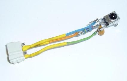
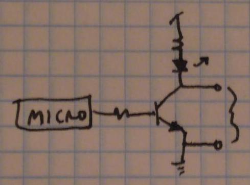
By the way - last time I noted a lot of random noise in the IR signal. I decided to build another IR module circuit (IR receiver, resistor, capacitor), this time with the components socketed, so I could more easily debug the problem. Lo and behold, the new circuit has no noise. At some point I'll disassemble the first IR module and swap its parts into the new circuit to see if I can blame the noise on a defective component, but for now, I'd rather do something more fun: decipher the Xbox remote codes.

First off, a fundamental fact about IR communication. The usual milieu for such communication is a noisy environment inhabited by naive yet fault-intolerant users. Transmission is expected to work perfectly, even if the batteries are weak and the user is pointing the remote at the wrong device. The IR receiver compensates for a lot of these problems in its cascade of analog circuits (here), and it performs admirably, but all that circuit can detect is full-on (mark) and full-off (space). So, for any given remote, for each of its buttons, a particular sequence of mark and space durations will be transmitted. The set of possible sequences, and their interpretation into data, is the protocol.

Long ago, before the Internets, I would have had to pore over traces of mark-and-space durations, seeking the elusive pattern of the protocol. Well! That would have been good clean fun. However, on the Internets I see that someone has already done that part. The Xbox remote allegedly conforms to the "RCA protocol". To summarize:

  • 4ms mark, 4ms space begins a transaction.
  • The data is in "pulse distance protocol": each bit consists of a 500μs mark, followed by either 1ms space (logical 0) or 2ms space (logical 1).
  • 24 bits are sent per transmission (4-bit address, 8-bit command, then complement of that same address and command).
  • Address and command are sent MSB-first.
  • Each transmission ends in a final 500μs mark.

I have some experimental data; how well does it match up with that description? Before I answer that question, I'm afraid I'm going to indulge myself in a little rant.

Signaltap's Tragic Flaw

I thought I had a great flow going here. My input was a handful of verilog files and a tcl script for each stage of the flow. I was making good progress (I thought) toward a data collection system which would work like this:

  1. I type "make" (or something)
  2. The fpga configuration file is built, if necessary (if any of its dependencies changed)
  3. The fpga is programmed from its configuration file
  4. I'm prompted, "type the name of a remote control button, then press that button, or <esc> to quit"
  5. I do it, and the signaltap data for that button is captured and logged
  6. After enough data logging, I type <esc> and data for each button is written to a report file.

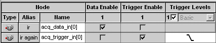
I can do everything up to step 5), but step 6) appears to be impossible! Why? When, via a tcl script, signaltap is instructed to capture data, the captured data goes into the stp file. (That file looks like some form of XML.) But there are no scripting commands (at least that I could discover) which make stp file data available for further processing. I'm sure I could figure out the format of the XML file and get the data, but that just seems deeply wrong. So sad.

Fallback position: The GUI does provide a way to export signaltap data into various formats. I'll convert my data using the GUI, then work on it in Excel. It'll work, but it will be very time-consuming. Oh, well.

Onward! An example: DISPLAY

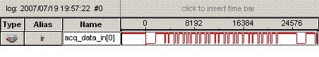
Is my Xbox remote really transmitting according to the RCA protocol? I'll have a look at the data that's transmitted when the DISPLAY button is pressed. Here's the sequence of pulse durations that occur, in milliseconds. (I admit to begging the question in the suspicious display format I've chosen.) The first pulse is a "mark" (active transmission, and logic low on the ir signal). Each subsequent number is the duration of a pulse of opposite type to its predecessor.

4,4,
0.5,1,0.5,2,0.5,1,0.5,2,
0.5,1,0.5,1,0.5,2,0.5,1,0.5,2,0.5,1,0.5,2,0.5,1,
0.5,2,0.5,1,0.5,2,0.5,1,
0.5,2,0.5,2,0.5,1,0.5,2,0.5,1,0.5,2,0.5,1,0.5,2,
0.5

Now, if I believe the RCA protocol description, each sequence "0.5,1" is a logical 0, and each "0.5,2" is a logical 1. And I can strip off the 4 ms mark-space at the beginning, and the terminal 0.5ms mark. The result:

0 1 0 1 
0 0 1 0 1 0 1 0 
1 0 1 0 
1 1 0 1 0 1 0 1 

As predicted, I see 12 bits (4 address, 8 command) and then their complements. Here's the beginning of a table:

Button Address (hex) Command (hex)
DISPLAY 5 2A

Next up: I'll fill in the rest of the table. There are 27 buttons on the Xbox remote - this will be tedious.

Postscript: I lied. The mark/space durations above matched the RCA protocol perfectly. But it just isn't true! Unless, that is, I quantize to 1 decimal place, as I did for the data above. If I look at my data with a higher-resolution lens, I see a less tidy picture. This table shows the discrepancies, which are accurate to one signaltap period (5.12μs):

Duration type Protocol prediction My measurement
Initial Mark 4ms 4.0448ms
Initial Space 4ms 3.9782ms
Bit-start Mark 0.5ms 0.5325ms
Logical-0 Space 1ms 0.9677ms
Logical-1 Space 2ms 1.9712ms

Here are some hypotheses which would explain the discrepancies:

  1. The author of the RCA protocol quantized to 1 decimal place.
  2. Xbox remotes are not particularly accurate - mine just happens to be a bit out of whack.
  3. Something in my experimental setup is introducing a systematic error into my measurements - notice that each "mark" value is slightly larger than expected, while each "space" value is slightly smaller.

Mulling over these hypotheses will give me something interesting to do while I go about the rote business of collecting and translating the data for the button-to-code table.

tb_5 files

August 18, 2007

XBox DVD Remote Control Codes

Here are the address and command codes for each of the XBox DVD Remote's 27 buttons.

Button Address (hex) Command (hex)
menu 5 08
play 5 15
pause 5 19
title 5 1A
forward 5 1C
reverse 5 1D
stop 5 1F
skip+ 5 20
skip- 5 22
back 5 27
display 5 2A
0 5 30
1 5 31
2 5 32
3 5 33
4 5 34
5 5 35
6 5 36
7 5 37
8 5 38
9 5 39
info 5 3C
left_arrow 5 56
right_arrow 5 57
down_arrow 5 58
up_arrow 5 59
select 5 F4

PS: 20070901: I happened upon a list of the Xbox remote codes, here. LIRC looks like a cool project.

August 20, 2007

Gathering the XBox DVD Remote Codes: Method

Last time I presented a table of address and command codes, one for each of the XBox DVD Remote's 27 buttons. How did I come up with the table?

First, a recap: back in X. Start Making Sense, I displayed disappointment at Signaltap's partial scriptability, and resigned myself to manually processing the data, in heavy interaction with Signaltap's GUI and Excel. This solution, though workable, didn't sit well with me, and fortunately I found a better method.

The Virtual JTAG Interface To The Rescue!

The sld_virtual_jtag megafunction, aka the Virtual JTAG interface (VJI), provides access to the same on-chip hardware resources that signaltap makes use of, but in a far more user-configurable form. Here's what the Mighty Altera Corporation says:

The megafunction can be used to diagnose, sample, and update the values of internal parts of your logic. With this megafunction, you can easily sample and update the values of the internal counters and state machines in your hardware device.

You can build your own custom software debugging IP using the Tcl commands listed above to debug your hardware. This IP communicates with the instances of the sld_virtual_jtag megafunction inside your design.

I used the VJI, suitably wrapped in glue logic, to gather data under control of a tcl script. I'll give a brief textual description of the method I used; check out the attached design files for more details.

Remember that my goal is to measure the durations of the mark and space values emitted by the remote control. The measurement circuit consists of these functional blocks:

  • An edge detector, which provides a 1-cycle pulse on each rising or falling edge of the incoming IR signal
  • A 20-bit counter, which increments on each clock pulse, and synchronously resets to 0 on each IR edge
  • A 20-bit FIFO, which is written with the counter value on each IR edge

Those simple circuit elements, running at 50MHz, write the sequence of IR duration values into the FIFO. The read side of the FIFO is controlled by the VJI, which exposes two values to the outside world:

  • rdempty: is the FIFO empty?
  • readdata: data from the FIFO

A tcl script (pseudo code, here - the actual script is get_data.tcl) running on the host gathers the FIFO data:

while (FIFO nonempty)
  read FIFO
  print FIFO readdata
end while

The script process_data.bat transforms data from all raw data files into a single summary file and one processed data file per raw data file. So, that's the basic operation of the data-acquisition logic. Next time I'll do some analysis on the gathered data.

Postscript: The testbench for this data acquisition fiesta is "tb_6"; here are the files. This testbench could actually be useful to anyone trying to analyze a serial protocol, so it's worthwhile to give a bit of an overview. The zip file contains these files:

  • go.sh: Build bash script. Creates the quartus project, compiles the design and configures the FPGA.
  • pgm.sh, make_tb.tcl, compile_tb.tcl: Lower-level build tcl scripts.
  • top.v: Design top-level. Synchronizes the incoming IR signal to the system clock, instantiates module "sys".
  • sys.v: The real guts of the design. Implements the edge detector, the counter and the FIFO. Instantiates the virtual jtag wrapper module (vj_rw). Drives the test bench code ("06.") onto the seven-segment display.
  • fifo.v: A dual-clock FIFO, delivered by the FIFO megawizard.
  • vj_rw.v: Assorted logic to provide a clean interface to the virtual-jtag-interface, from the outside world. Instantiates the virtual-jtag-interface itself (vj).
  • vj.v: The actual virtual-jtag-interface, as delivered by the virtual jtag interface megawizard.
  • get_data.tcl: The data acquisition script, as described above. Reads the FIFO, writes the values to the console, slightly formatted (newlines are inserted for "long" durations, which are supposed to be IR transmission boundaries
  • process_data.bat: A perl script which transforms the raw data (as delivered by get_data.tcl) into "cooked" data files, a summary file of IR codes, and an html table for pasting here. This file is very XBox-remote-specific.

August 26, 2007

WWASD?

I've got the data from hundreds of remote-control transmissions in a handy file format. What would a statistician do? Analyze it, of course!

Remember that the XBox remote transmits in the RCA protocol; that protocol allows for 5 different sorts of pulses:

  • mark_4ms: nominal 4 ms "mark" (active IR transmission)
  • space_4ms: nominal 4ms "space" (no IR transmission)
  • mark_500us: nominal 500μs mark
  • space_1ms: nominal 1ms space (logic 0)
  • space_2ms: nominal 2ms space (logic 1)

The real world is usually a bit messy - in this particular case, the data I measured coming out of the IR receiver module diverges from those nice values. So, by trial and error, I determined an upper and lower bound for each pulse type. I bin the data into the 5 types according to these thresholds (a value falls in a bin if it is in the range (min-bin-value, max-bin-value), where the parens represent noninclusive boundaries):

bin min-bin-value max-bin-value
mark_4ms 4.01 4.07
space_4ms 3.9 4.0
mark_500us 0.5 0.56
space_1ms 0.9 1.0
space_2ms 1.94 2.0

Notice that the "mark" bins have larger than nominal values, while the "space" bins have smaller than nominal values. (By the way, by design, every duration value I collected falls into one of the 5 bins.)

Here are some statistics on the collected data, grouped by bin:

bin average value min value max value deviation from nominal (%) number of samples
mark_4ms 4.046216011 4.02744 4.06724 +1.155% 1514
space_4ms 3.979702576 3.96054 3.99844 -0.507% 1514
mark_500us 0.539785722 0.51732 0.55442 +7.957% 37850
space_1ms 0.95811015 0.94466 0.98132 -4.189% 18168
space_2ms 1.965947435 1.94998 1.98714 -1.703% 18168

Average, min and max are useful, and reveal basic facts, but also hide other things. For a full picture, there's nothing like... a picture. I discovered something interesting when I plotted each bin's data as a histogram. Click on a chart thumbnail to see the full-size version:

IR Receiver Output

Bin Histogram
mark_4ms
space_4ms
mark_500us
space_1ms
space_2ms

Isn't that peculiar? The data for each bin is clustered into groups rather than being a nice normal distribution.

Well. The measurement is made on the output of the IR receiver; could that receiver be distorting my nice clean data? Moving upstream a bit, I took apart the Xbox remote control, and found a very simple circuit driving the IR LED. (The box labled "micro" is an integrated circuit whose markings were pretty much indecipherable - presumably some simple microcontroller.)

measurement3.jpg

I've taken a new set of measurements between the cathode of the IR LED and ground.

Internal-toXBox-Remote, IR cathode-to-ground

Bin Histogram
mark_4ms
space_4ms
mark_500us
space_1ms
space_2ms

These histograms show that the XBox remote itself is emitting pulse durations which tend to cluster into sub-bins separated by about 20μs. The histograms have higher peaks than those measured at the IR output - perhaps the IR receiver circuit has a "smearing" effect (I can imagine that the automatic gain-control part of the receiver would have this effect).

Move forward!

This measurement and analysis is fun laboratory work, but I'm anxious to get started on some firmware. Were I to continue in this vein, I'd work on some of these tasks:

  • Investigate the effect of transmitter-to-receiver distance on pulse durations
  • Get at least one more Xbox remote, and compare pulse duration statistics
  • Try to find a datasheet for the alleged microcontroller in the Xbox remote
  • Probe more pins on the alleged microcontroller - try to correlate pulse duration with power supply, incoming clock frequency, ...

But instead, now it's time to get back to my long-neglected f2013. As a preliminary step, I plan to learn about the f2013's clock source options think about the problem of debugging visibility in embedded systems.

Oh, right. Here are the up-to-date tb_6 (IR receiver measurement) and tb_7 (IR LED cathode measurement) files.

September 13, 2007

Hello, world!

It's finally time to work on some firmware!

But, since I seem to be compelled to develop a design environment rather than actually work on a design (what was I working on? Something about turning something on, or off... something like that), let's talk about debugging tools. Well. Let's talk about bugs, first.

Bugs that, say, the compiler fails on, are simple: they're right there in red text. Those bugs die quickly. (Are these even bugs? Perhaps not. But I'll assume they are, for the sake of my point.) On the other end of the spectrum are those extremely intermittent bugs which seem to occur only when we're not looking. We know these bugs through stale logfile tracings, collections of disproven hypotheses, and a body of murky, often contradictory and superstitious lore which grows throughout the long, long lifespan of the bug.

Bugs elude us by hiding. So, what do I want from a debugging tool? I wouldn't ask for too much - just something which:

  • is no more difficult to use than it ought to be
  • lets me see everywhere
  • has no effect on the normal operation of the system
  • lets me gather trace data on the workings of the system, in its actual working environment
  • provides a way to inject artificial stimulus into the system, for testing purposes

I do have a few debugging tools handy. How do they rate?

  • LEDs. These are very easy to use: write a value, look at the blinky lights. LEDs can answer questions like:
    • Is it on?
    • Is it the correct version (like my testbench id on the 7-segment display)?
    • Is it toggling? (At human-perceptible rate, at least.)
    But the amount of information you can transmit to a human via LED is limited, and you very quickly yearn for more.
  • The IAR IDE debugger. Single-stepping through your program is a great way to find dumb errors. Breakpoints are available too. This is a very user-interface-intensive debugging methodology, though, and can dramatically affect program execution time, leading to the dreaded Heisenbug.
  • Signaltap(tm). Signaltap can show me anything happening inside the FPGA (so, in my little rig, anything on the f2013 pins), and can capture a trace of that data, sampled on any clock I choose. This is great stuff! But, it's kind of a pain in the neck to set up, and the penalty for the frequent "I just want to see one more thing" moments in debugging is usually a hardware recompile. Signaltap is not suited to a pure scripted flow, since trace data is stowed in an undocumented file format. The amount of data that can be captured is limited to what fits in the onchip memory.
  • Custom logic using the sld_virtual_jtag. Think of this as a hand-crafted signaltap, accessible via tcl script. This answers the scripting flow problem of signaltap. Captured data size is unlimited, as long as the bandwidth out of the jtag link is sufficient to keep up with the data generation rate. The information flow can go the other way, too: the system-under-observation's inputs can be driven from the custom logic, ultimately from a script running on the host, which opens up an interesting world of test possibilities. Naturally this more powerful debugging tool is even more work to set up than signaltap, since you have to design the custom logic and write scripts to access the link.

So, it looks like I'm a little heavy on the powerful-but-hard-to-use side. What I'm missing is something simple and quick to iterate on, which can give me lots of data without burdening the system too much. What I need is something like... printf.

Something like printf

Most microcontrollers have some form of built-in serial communications module. The f2013 is a bit odd: rather than a plain-ol' UART, its communications module speaks SPI or I2C. But that's ok - my laptop doesn't have a UART either. Fortunately, to assist me in the simple goal of streaming bytes from the f2013 to my laptop under firmware control, I have a giant heap of programmable logic right next to my f2013, which I can use to bridge the gap between the f2013 and the laptop. Think of the solution as an "SPI-to-JTAG bridge". Here's a block diagram showing the path of a byte from f2013 to laptop:

block_tb8.gif

The components of the system are:

  • The f2013, configured with an 8-bit SPI master
  • The 1c20, configured with
    • An 8-bit SPI slave
    • A DMA component, configured to (forever) read bytes from the SPI slave and write them to...
    • A "JTAG UART"
  • The USB Blaster (the same device that I use for downloading sofs, running signaltap, etc.
  • The terminal program nios2-terminal, running on the host computer

Say, not to pull a fast one: I realize that this is the first time I'm using a system which consists of other than hand-typed Verilog and the odd megafunction module. I designed this system using Altera's SOPC Builder, which you can think of as a heap of useful hardware components and an automatic bus generator. The system consumes 303 logic elements - pretty small. For reference, tb_6, my most complex system so far, consumed 312 LEs. SOPC Builder generation and Quartus compilation complete in about 2.5 minutes.

For anyone reading who happens to be familiar with SOPC Builder, I used these tricks to optimize the system for low logic consumption and fast generation:

  • The DMA's registers are reset to an actively-running state, so that I don't need a complicated master to configure the DMA at run-time. I used an undocumented feature of the DMA for this trick, which, sadly, requires running in "--classic" mode
  • I set the DMA's internal FIFO depth to 1 location (another undocumented feature)
  • I limited the DMA to performing 8-bit transactions
  • I reduced the JTAG UART FIFO transmit and receive FIFO depths to minimal values

f2013 firmware This is a pretty simple firmware project: all I'm doing is sending a string of bytes, over and over, so I can see it in the terminal program. It took a bit of research to hit upon the correct combination of control register values; see utility routines init_spi and send_spi in the attached project archive.

By the way, I have to create my own SPI chipselect (SS_n), using a generic f2013 pin, since the built-in SPI master doesn't provide that automatically. Also notice that send_spi is a polling transmit routine: clearly the next step is to create an IRQ-based transmitter.

Hello, world!

Here's a screen capture of the spi test firmware in action:

nios2-terminal.gif

P.S. The bug is in the pin assignments

For my own reference, mostly, here's a table of pin names and functions for this little test bench:

f2013 function f2013 SPI function 1c20 pin J15 pin
P1.4 <none> U11 J15-12
P1.5 SCLK Y11 J15-14
P1.6 MOSI W11 J15-13
P1.7 MISO V11 J15-11

Here's the tb_8 archive.

20070922: a small optimization: SOPC Builder's DMA is a bit overpowered for the simple task of moving bytes from one place to another. Also, needing to use undocumented features annoys me. It was about a half hour's work to create a new component (simple_byte_pipe) that does the same job, wiith less logic. The new system (files attached as tb_8a.zip) uses only 248 LEs, and builds in 1.5 minutes.

tb_8a archive.

November 25, 2007

Pulse Measurement Testbench

The heart of an IR receive circuit is the pulse measurement circuit. A single-bit signal goes in, and the length of each input pulse goes out. IR-protocol-specific logic to decode the actual data values being transmitted would work off the sequence of length values coming out of the pulse measurement block. The pulse-measurement circuit itself, though, is protocol-agnostic.

Now, I'm planning to build this pulse-measurement circuit (and later on, the follow-on data decode circuit) in firmware in the f2013. I could drive pulses into the f2013 by aiming an IR remote control at the IR transceiver (as seen in VIII. My Little GP1UE267XK) and pushing various buttons on the remote. That sounds pretty annoying - I'd have to pick up and put down the remote all the time, in between typing, and the resulting pulses would vary in length according to factors beyond my control (as I documented in XIII. WWASD?).

Here's a better idea: I'll build logic in the FPGA to generate precise, reproducible pulse sequences, under control of the host PC. Without moving my hands from the keyboard, I'll download various pulse sequences to the hardware, which in turn will drive the device-under-test (f2013 firmware in active development). If I equip the f2013 and testbench logic with a SPI-to-JTAG bridge (as seen in XIV. Hello, world!), then the f2013 can send its interpretation of the pulse sequence back to the host. A script can compare the f2013's report with what was sent - so - a regression test system is possible.

Here's a top-level block diagram of the system:

block.gif

You can see three basic sub-blocks:

  1. VJI: A virtual-JTAG-interface which provides a FIFO-write interface ("source") and an additional signal, "go".
  2. Pulse Gen: The pulse generator proper. The idea here is that the VJI writes a sequence of values into the pulse generator's internal FIFO (data rate limited by the JTAG interface), then asserts the "go" signal, which initiates processing on the FIFO data at top speed. Data read from the internal FIFO specifies the level and pulse duration on the single-bit output, "out".
  3. f2013: The f2013 hardware/software block, which is the real device-under-test here, y'all. The f2013 will measure successive pulse durations and (at least for test purposes) transmit the pulse length values via SPI back to the host.

Notice symmetry: the testbench in XII. Gathering the XBox DVD Remote Codes: Method transformed sequences of pulses from the IR remote into sequences of pulse durations. The new testbench will do the inverse transformation, durations to pulses. I have a big pile of labeled sample data which I collected during the IR remote protocol analysis; I can "play back" the samples to the f2013 firmware as I develop it.

Alright then. For the implementation, I'll generate the entire FPGA system (quartus project, pinout declarations and HDL) via script, relying heavily on europa_module_factory. The next step will be to flesh out the sub-sub-blocks within the VJI and Pulse Gen sub-blocks.

December 24, 2007

vji_component

To continue!

I've created a new component, vji_component. In the planned pulse measurement testbench, this component will be the bridge between the host system and the pulse generator logic. The general purpose of vji_component is to provide one or more host-accessible input or output signals, while hiding all the complexity of using the sld_virtual_instance.

For components I've written previously, I've provided a handful of test cases. These test cases were simple: each one generates a particular instance of the component, and then compares the generated HDL against a "known good" reference HDL file. One problem with this approach is that my "known good" files have not actually been verified for correct function. Still, this method lets me proceed confidently with component changes which should not result in changed output. vji_component follows the same basic flow that I've established with previous components, but with one additional test feature: a system test.

In the system test, a vji_component instance is configured to have an input and output signal of width 24 (by default; the width is configurable). The output signal wires to the input signal through inverters. A tcl script drives random numbers into the writedata port, reads back the inverted signal on the readdata port, and verifies the value. The block diagram shows what's going on (sorry about that "inv" block - my attempt at an ASCII inverter symbol ended in failure).

vji_component_system_test_block.gif

With this new system test, I'm taking the opportunity to create the entire system from as few source files as possible, under control of a Makefile. The system top-level is generated by a europa_module_factory-derived perl module and looks exactly like any other component. (I have come to realize that my use of the word "component" is not standard. When I say "component" I just mean some logic with optional sub-instances. Just about any HDL hierarchy is a "component", so maybe I need a different word.)

The test system source files are as follows:

  • make_quartus_project.tcl: creates the quartus project, makes pin assignments, etc.
  • vji_test_system/vji_test_system.pm: perl module for the system "component". One parameter is provided, "datawidth"
  • compile_quartus_project.tcl: compiles the project in quartus
  • test.tcl: functional test: a script to write, read and verify
  • Makefile: targets are:
    • qp: call a tcl script to create the quartus project
    • hdl: create the HDL
    • sof: compile to bitstream (sof)
    • pgm: program the FPGA
    • test: test the system by writing, reading and verifying
    • clean: destroy the evidence

The upshot of all this: 5 source files encode the system and test scripts. Typing "make" runs everything and reports any errors.

Zip archive of the vji_component and associated tests.

About XBox Remote Project

This page contains an archive of all entries posted to Aaron's Sandbox in the XBox Remote Project category. They are listed from oldest to newest.

Many more can be found on the main index page or by looking through the archives.

Powered by
Movable Type 3.31