To work! Here are the bits and pieces I'll be playing with:
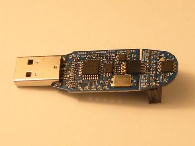
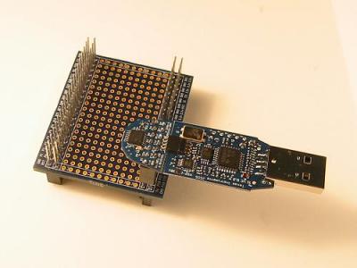
(I'll call it the "f2013" from now on.) The f2013 has 14 through-holes in the tiny board which contains the microcontroller. These 14 pins connect directly to the 14 pins of the microcontroller. The f2013 as shipped is inside a plastic case; with a little care it's easy to pry apart the two halves of the case to get access to the f2013 board. Notice that I've soldered a 2x7 connector to the proto holes in the f2013.
Pins of the connector are labeled according to the micro pin they connect to, for example "P3" connects to microcontroller pin 3. The pins are physically arranged like this, if you're looking at the top view of the board (looking at the the connector pins as they are soldered into the through holes) with the USB connector on the left:
| P14 | P1 |
| P13 | P2 |
| P12 | P3 |
| P11 | P4 |
| P10 | P5 |
| P9 | P6 |
| P8 | P7 |
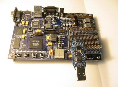
1c20 board (links to pdf)
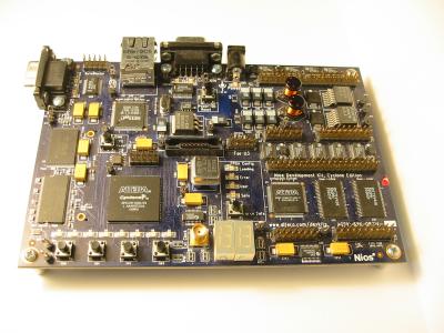
This is a development board for a perfectly decent, but rather old FPGA - the Cyclone 1c20. Since I work for Altera, it's easy for me to get my hands on one of these boards. I chose this board because it still works just fine with modern tools. Any dev board with a santa cruz connector would work equally well.
J15 is a handy 14-pin connector in a 2x7 arrangement, just right for plugging the f2013 into. Well. Almost just right. More below. Here's the pinout:
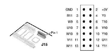
If I blindly plugged the f2013 into J15, these are the connections that would result:
| J15 pin | J15 function | f2013 pin | f2013 function |
|---|---|---|---|
| J15-1 | GND | P14 | GND |
| J15-2 | +5V | P1 | VCC |
| J15-3 | R11 | P13 | XIN |
| J15-4 | Y9 | P2 | P1.0 |
| J15-5 | W9 | P12 | XOUT |
| J15-6 | T10 | P3 | P1.1 |
| J15-7 | U10 | P11 | TEST |
| J15-8 | V10 | P4 | P1.2 |
| J15-9 | W10 | P10 | RST |
| J15-10 | Y10 | P5 | P1.3 |
| J15-11 | V11 | P9 | P1.7 |
| J15-12 | U11 | P6 | P1.4 |
| J15-13 | W11 | P8 | P1.6 |
| J15-14 | Y11 | P7 | P1.5 |
The problem is on the second line of the table: J15-2 is +5V, but the f2013 VCC is only 3.6V. Bad things will happen if I connect those two power supplies! I could physically remove that pin of the 2x7 header soldered to the f2013, but in the ultimate application, that pin may be used for supplying power. Or, I could cut the +5V pin on J15, but I don't really want to modify the 1c20 board. Solution: don't plug the f2013 directly into the 1c20 board; instead, plug it in via an intermediate board, which will connect every pin except for J15-2/P1.
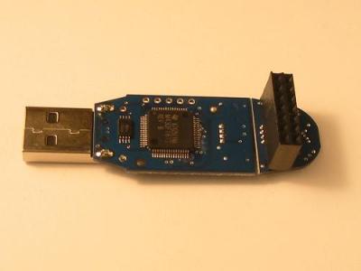
Santa Cruz Connector Prototype Board
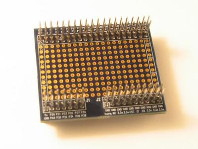
This is a handy little prototype board which plugs into the "santa cruz connector" footprint of the 1c20 board. I've carved away the connection of J15-2, so that the 1c20 board's +5 supply doesn't connect to the board. The f2013 board connects right into the santa cruz board:
And then the santa cruz board plugs into the 1c20 board:
That's enough for now - next time, I'll cover the process of building a testbench, a.k.a. a binary configuration file for the FPGA.
Comments (1)
Ok. Now I finally understand. That's a pretty brillig little system for peeking, poking, and generally prodding the dut!
Posted by david van brink | June 18, 2007 8:48 PM
Posted on June 18, 2007 20:48