« August 2007 | Main | October 2007 »

September 2007 Archives

September 13, 2007

Hello, world!

It's finally time to work on some firmware!

But, since I seem to be compelled to develop a design environment rather than actually work on a design (what was I working on? Something about turning something on, or off... something like that), let's talk about debugging tools. Well. Let's talk about bugs, first.

Bugs that, say, the compiler fails on, are simple: they're right there in red text. Those bugs die quickly. (Are these even bugs? Perhaps not. But I'll assume they are, for the sake of my point.) On the other end of the spectrum are those extremely intermittent bugs which seem to occur only when we're not looking. We know these bugs through stale logfile tracings, collections of disproven hypotheses, and a body of murky, often contradictory and superstitious lore which grows throughout the long, long lifespan of the bug.

Bugs elude us by hiding. So, what do I want from a debugging tool? I wouldn't ask for too much - just something which:

  • is no more difficult to use than it ought to be
  • lets me see everywhere
  • has no effect on the normal operation of the system
  • lets me gather trace data on the workings of the system, in its actual working environment
  • provides a way to inject artificial stimulus into the system, for testing purposes

I do have a few debugging tools handy. How do they rate?

  • LEDs. These are very easy to use: write a value, look at the blinky lights. LEDs can answer questions like:
    • Is it on?
    • Is it the correct version (like my testbench id on the 7-segment display)?
    • Is it toggling? (At human-perceptible rate, at least.)
    But the amount of information you can transmit to a human via LED is limited, and you very quickly yearn for more.
  • The IAR IDE debugger. Single-stepping through your program is a great way to find dumb errors. Breakpoints are available too. This is a very user-interface-intensive debugging methodology, though, and can dramatically affect program execution time, leading to the dreaded Heisenbug.
  • Signaltap(tm). Signaltap can show me anything happening inside the FPGA (so, in my little rig, anything on the f2013 pins), and can capture a trace of that data, sampled on any clock I choose. This is great stuff! But, it's kind of a pain in the neck to set up, and the penalty for the frequent "I just want to see one more thing" moments in debugging is usually a hardware recompile. Signaltap is not suited to a pure scripted flow, since trace data is stowed in an undocumented file format. The amount of data that can be captured is limited to what fits in the onchip memory.
  • Custom logic using the sld_virtual_jtag. Think of this as a hand-crafted signaltap, accessible via tcl script. This answers the scripting flow problem of signaltap. Captured data size is unlimited, as long as the bandwidth out of the jtag link is sufficient to keep up with the data generation rate. The information flow can go the other way, too: the system-under-observation's inputs can be driven from the custom logic, ultimately from a script running on the host, which opens up an interesting world of test possibilities. Naturally this more powerful debugging tool is even more work to set up than signaltap, since you have to design the custom logic and write scripts to access the link.

So, it looks like I'm a little heavy on the powerful-but-hard-to-use side. What I'm missing is something simple and quick to iterate on, which can give me lots of data without burdening the system too much. What I need is something like... printf.

Something like printf

Most microcontrollers have some form of built-in serial communications module. The f2013 is a bit odd: rather than a plain-ol' UART, its communications module speaks SPI or I2C. But that's ok - my laptop doesn't have a UART either. Fortunately, to assist me in the simple goal of streaming bytes from the f2013 to my laptop under firmware control, I have a giant heap of programmable logic right next to my f2013, which I can use to bridge the gap between the f2013 and the laptop. Think of the solution as an "SPI-to-JTAG bridge". Here's a block diagram showing the path of a byte from f2013 to laptop:

block_tb8.gif

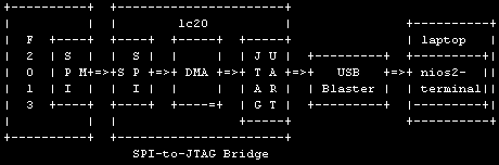
The components of the system are:

  • The f2013, configured with an 8-bit SPI master
  • The 1c20, configured with
    • An 8-bit SPI slave
    • A DMA component, configured to (forever) read bytes from the SPI slave and write them to...
    • A "JTAG UART"
  • The USB Blaster (the same device that I use for downloading sofs, running signaltap, etc.
  • The terminal program nios2-terminal, running on the host computer

Say, not to pull a fast one: I realize that this is the first time I'm using a system which consists of other than hand-typed Verilog and the odd megafunction module. I designed this system using Altera's SOPC Builder, which you can think of as a heap of useful hardware components and an automatic bus generator. The system consumes 303 logic elements - pretty small. For reference, tb_6, my most complex system so far, consumed 312 LEs. SOPC Builder generation and Quartus compilation complete in about 2.5 minutes.

For anyone reading who happens to be familiar with SOPC Builder, I used these tricks to optimize the system for low logic consumption and fast generation:

  • The DMA's registers are reset to an actively-running state, so that I don't need a complicated master to configure the DMA at run-time. I used an undocumented feature of the DMA for this trick, which, sadly, requires running in "--classic" mode
  • I set the DMA's internal FIFO depth to 1 location (another undocumented feature)
  • I limited the DMA to performing 8-bit transactions
  • I reduced the JTAG UART FIFO transmit and receive FIFO depths to minimal values

f2013 firmware This is a pretty simple firmware project: all I'm doing is sending a string of bytes, over and over, so I can see it in the terminal program. It took a bit of research to hit upon the correct combination of control register values; see utility routines init_spi and send_spi in the attached project archive.

By the way, I have to create my own SPI chipselect (SS_n), using a generic f2013 pin, since the built-in SPI master doesn't provide that automatically. Also notice that send_spi is a polling transmit routine: clearly the next step is to create an IRQ-based transmitter.

Hello, world!

Here's a screen capture of the spi test firmware in action:

nios2-terminal.gif

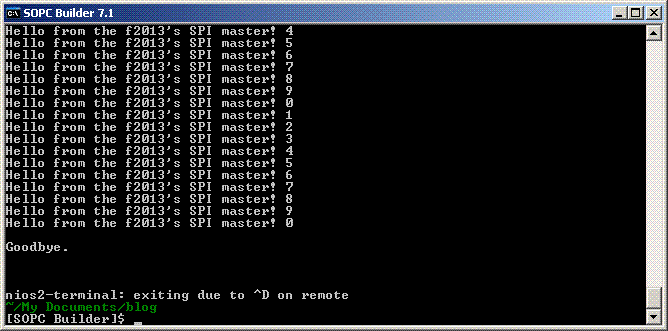
P.S. The bug is in the pin assignments

For my own reference, mostly, here's a table of pin names and functions for this little test bench:

f2013 function f2013 SPI function 1c20 pin J15 pin
P1.4 <none> U11 J15-12
P1.5 SCLK Y11 J15-14
P1.6 MOSI W11 J15-13
P1.7 MISO V11 J15-11

Here's the tb_8 archive.

20070922: a small optimization: SOPC Builder's DMA is a bit overpowered for the simple task of moving bytes from one place to another. Also, needing to use undocumented features annoys me. It was about a half hour's work to create a new component (simple_byte_pipe) that does the same job, wiith less logic. The new system (files attached as tb_8a.zip) uses only 248 LEs, and builds in 1.5 minutes.

tb_8a archive.

September 27, 2007

SPI Makeover: Mission Statement

Time for another distracting tangent. The tb_8 system consists of:

  1. a JTAG UART (104 LEs)
  2. my little custom byte-pipe (9 LEs)
  3. an 8-bit SPI slave (40 LEs)

The first two components are beyond reproach: the JTAG UART because I have no idea how it works, but it works, and my little byte-pipe because it's so cute and tiny.

But the SPI slave; that's another matter. My feeling upon reading the HDL implementation, spi.v, is that its designer was not only criminally incompetent, but also completely disinterested in producing legible code. And maybe 40 LEs is not so much, but I believe I can do better. Also, in the process of doing this reimplementation, I can write a few words on my favorite hardware design methodology, "Europa".

To wrap up, here are the metrics by which I'll judge the existing spi.v versus my new implementation, in priority order:

  • Proper function
  • HDL readability
  • Configurability. I'm thinking I need to support both flavors of clock polarity and clock phase, and also various data widths.
  • FPGA resource consumption
  • There you have it. The challenge is on!

September 29, 2007

A Flash of Inspiration: Useless Features are Bad

The Altera-provided SPI slave component is configurable in several ways:

  • Data format: MSB-first or LSB-first
  • Data width: 1 to 16 bits
  • Clock polarity (CPOL): non-inverted or inverted
  • Clock phase (CPHA): leading or trailing edge sample

(The data-related stuff is obvious; see Wikipedia for a decent explanation of CPOL and CPHA.)

I see a way to make my task easier: drop configurable CPOL and CPHA. That sort of configurability in an SPI slave is a useless feature, and I can prove it. First, consider this fact: most existing SPI slaves lack CPHA and CPOL configurability. (Imagine a cheap SPI-equipped ADC chip. If it were configurable, how would you configure it? By tying pins high or low? Too expensive. By init-time communication via secret codes from the SPI master? Well, I'm sure you see the problem with that idea.) Because there are exist non-configurable SPI slaves, SPI masters (like the one in the f20123) must pick up the slack and provide variable CPHA and CPOL. There's no value in making both ends of the link configurable, so I'll drop that bit of needless complexity and choose CPOL=0, CPHA=0 for my new SPI slave.

That's a relief. Fewer features means less complexity, fewer bugs, easier testing. So, what features do I deem useful enough to implement?

  • Data width: 1 up to some huge number, why not.
  • MSB-first or LSB-first data
  • Proper operation if SS_n is tied low (in other words, don't rely on SS_n falling or rising edges). But do resynchronize on inactive SS_n, if it occurs.
  • Double-buffered transmit and receive registers
  • Avalon-ST source and sink interfaces, or Avalon-MM slave interface with flow control
  • Verilog or VHDL implementation, which must be at least barely human-readable

That'll do. Next time: some block diagrams.

September 30, 2007

Block Diagrams? Well, Block Descriptions.

I don't have a usable block diagram editor. I tried Microsoft Paint, but it's too bitmap-oriented. I have used Quartus successfully for simple diagrams, but it's not very flexible. I think I achieved the limit of the ASCII block diagrams a while back. So, for now, I'll describe my blocks in words. If anyone has a suggestion for a free and decent block diagram editor, please let me know!

Here are the sub-blocks of the SPI Slave implementation, which will map directly to HDL modules:

  • sync: this block synchronizes the SPI input signals to the system clock domain. Nothing fancy here; just the traditional chain of 2 flip flops, which I use as a magic talisman to ward off metastability.
  • sequencer: From the synchronized SCLK signal (sync_SCLK), this block produces two active-high event triggers:
    1. shift: enable a shift on the outgoing data shift register
    2. sample: enable a sample of the incoming data
    (If I wanted to create a CPOL- and CPHA-configurable slave, this block is the only one that would change.)
  • bit_counter: for a n-bit SPI slave, this block counts from 0 to n-1, incrementing once for each shift. Its outputs control some FIFOs (see below). Inactive level (high) on SS_n resets this counter to 0.
  • rx: MOSI feeds an n-bit shift-register chain, enabled by shift.
  • rx_fifo: A basic FIFO with clk, write, writedata, read, readdata, full and empty signals. When not empty, readdata is valid. For this FIFO, writedata is the rx shift-register chain. For now, this FIFO has a single storage element - call it a receive holding register, if you like. In the future, more FIFO locations may be useful; if so, this block's interface need not change.
  • av_st_source: input is the rx_fifo outputs; output is a standard set of signals implementing an Avalon ST source. This block is just wires.
  • tx: a parallel-loadable shift register. The shift-register output drives MISO directly.
  • tx_fifo: Another FIFO. This one drives the parallel-load input on tx, and accepts data from the Avalon-ST sink or Avalon-MM interface.
  • av_st_sink: another just-wires block. Avalon-ST is pretty much designed to bolt up directly to FIFOs, and this one connects to tx_fifo.
  • av_mm_slave: this optional block funnels the Avalon-ST interfaces into a single Avalon-MM slave interface with flow control (readyfordata, dataavailable). It'll take some careful thought to avoid deadlock on this interface. The lock-step full-duplex nature of SPI will be a key factor in this.

That seems like a lot of blocks! Fortunately, though, most of them are very very simple.

Next, I'll get to dig into the implementation. I'll probably need to say some introductory words about Europa, first.

A Note on Clock-Domain Crossing

I've made the choice to synchronize the SPI input signals as they enter the FPGA; all logic in the SPI slave will be in the system clock domain. Delaying the SPI signals like this implies an upper bound on the SCLK frequency, relative to the system clock rate (I think the max SCLK will be something like 1/4 the system clock frequency). There is another option: SCLK could drive a subsection of the SPI slave, all the way from serial input to parallel output. The parallel output would connect to proper clock-crossing FIFOs. This solution would be more complex, but should be able to run at a higher clk/SCLK ratio. I won't implement this solution for now, but it's worth keeping in mind if higher bandwidth is needed.

About September 2007

This page contains all entries posted to Aaron's Sandbox in September 2007. They are listed from oldest to newest.

August 2007 is the previous archive.

October 2007 is the next archive.

Many more can be found on the main index page or by looking through the archives.

Powered by
Movable Type 3.31