Main | July 2007 »

June 2007 Archives

June 9, 2007

Motivationally Speaking

Long ago, I used to make simple blinkin' LEDs projects using Microchip PIC devices. I had a cheap programmer, accessed over the parallel port, and the requisite set of simple tools from the manufacturer. It was all perfectly adequate for good clean LED fun. Lately, I've been feeling nostalgic for these simple projects. I want to make some simple hardware, and write simple software to make it go. While I'm making the project, I'll try out this new-fangled habit of keeping records in a publicly-accessible location, just in case 1) someone out there finds my notes useful and 2) the process forces me to usefully document the project for myself.

But! Time has passed. My PIC programmer is somewhere in deep storage, and my current computer doesn't even have a a parallel port. It's time to upgrade, and it looks like while I wasn't paying attention, some nice microcontrollers, complete with C compiler, showed up.

So here's my plan:

Mission: make the wonderful eZ430-F2013 do something cool. That sounds good, but too abstract, therefore:
More-Specific Mission: Add IR-remote-accesible turn-on function to my Xbox. I upgraded an ebay-procured Xbox with Xbox media center, and I like it, but the box can't be turned on via the remote when it's off. This problem has already been solved here, but I think I'd like to do it myself.
Less-Specific More-Specific Mission: During the design phase, think carefully about how to make the hardware and software modular, for a reusable platform. Some interesting module boundaries:

  1. IR carrier frequency module
  2. IR protocol module
  3. Exec module (what action(s) to take upon receipt of specific IR codes)

Development environment: I've previously only done the simplest of projects using the F2013. Working with a new microcontroller is process of exploration - learning how to configure the various hardware peripherals can be a matter of trial and error - the best way to get familiar is to fool around with it. To streamline that process, I'm going to embed my F2013 in a 1C20 development board, for complete control of all the pins and logic-analyzer function, all without touching a wire. Then I can create and download a new testbench environment over one USB cable, and compile and download new software to the F2013 over another.

June 14, 2007

The Bad Old Way

The standard procedure for developing a simple microcontroller project used to be:


  1. Get the testbench ready with power supplies, scope and any required signal sources

  2. Grab the breadboard and the handy collection of already-stripped 22GA wire

  3. Straighten the micro's pins and plug it into the breadboard, along with any LEDs, buttons or other stuff needed for the project

  4. Start code development. The last time I was doing this, the cycle was

    1. Write some code

    2. Grab a blank device from the UV eraser

    3. Plug it into the programmer's ZIF socket and program it

    4. Put the programmed part on the breadboard, and try it out

    5. Notice bugs, return the chip to the UV eraser. While the device is being erased, come up with ideas for how to fix the bug

    6. Back to the start!


Things are simpler now: there's no need for UV erasers, for one thing. The tools are better too: rather than instrumenting the code to transmit state information over a UART, or blink LEDs at specific execution points, just single-step through the code in the IDE. Still, it's not perfect. Here's my simplest-possible project, which makes an LED throb from full bright to full dark over several seconds:

breadboard.JPG

There are a few good things I can say about this method: it's simple and cheap. But mostly I don't like it: there's too much physical manipulation of wires and chips; it's too easy to accidentally destroy something; I'm always running out of the right kind of wire, the breadboard contacts wear out; hooking up scope probes is always troublesome - they seem to be carefully designed to rotate and jump off their clip point, then fall to the floor, dragging the breadboard with them - anyway, you can only probe the points which happen to be wired out to pins; creating a custom signal source which, say, mocks up some aspect of the application, for testing or analysis, probably means finding another breadboard to wire up, since the first one fills up quickly.

Of course I wouldn't be complaining about all this so much if I didn't have a solution in mind. Next: a better way.

June 16, 2007

Loomings

To work! Here are the bits and pieces I'll be playing with:

EZ430-F2013

ez430_f2013_top.jpg

ez430_f2013_bottom.jpg

(I'll call it the "f2013" from now on.) The f2013 has 14 through-holes in the tiny board which contains the microcontroller. These 14 pins connect directly to the 14 pins of the microcontroller. The f2013 as shipped is inside a plastic case; with a little care it's easy to pry apart the two halves of the case to get access to the f2013 board. Notice that I've soldered a 2x7 connector to the proto holes in the f2013.

Pins of the connector are labeled according to the micro pin they connect to, for example "P3" connects to microcontroller pin 3. The pins are physically arranged like this, if you're looking at the top view of the board (looking at the the connector pins as they are soldered into the through holes) with the USB connector on the left:

P14P1
P13P2
P12P3
P11P4
P10P5
P9P6
P8P7


1c20 board (links to pdf)

1c20_board.jpg

This is a development board for a perfectly decent, but rather old FPGA - the Cyclone 1c20. Since I work for Altera, it's easy for me to get my hands on one of these boards. I chose this board because it still works just fine with modern tools. Any dev board with a santa cruz connector would work equally well.

J15 is a handy 14-pin connector in a 2x7 arrangement, just right for plugging the f2013 into. Well. Almost just right. More below. Here's the pinout:

j15.GIF


If I blindly plugged the f2013 into J15, these are the connections that would result:

J15 pinJ15 functionf2013 pinf2013 function
J15-1GNDP14GND
J15-2+5VP1VCC
J15-3R11P13XIN
J15-4Y9P2P1.0
J15-5W9P12XOUT
J15-6T10P3P1.1
J15-7U10P11TEST
J15-8V10P4P1.2
J15-9W10P10RST
J15-10Y10P5P1.3
J15-11V11P9P1.7
J15-12U11P6P1.4
J15-13W11P8P1.6
J15-14Y11P7P1.5

The problem is on the second line of the table: J15-2 is +5V, but the f2013 VCC is only 3.6V. Bad things will happen if I connect those two power supplies! I could physically remove that pin of the 2x7 header soldered to the f2013, but in the ultimate application, that pin may be used for supplying power. Or, I could cut the +5V pin on J15, but I don't really want to modify the 1c20 board. Solution: don't plug the f2013 directly into the 1c20 board; instead, plug it in via an intermediate board, which will connect every pin except for J15-2/P1.

Santa Cruz Connector Prototype Board

sc_board.jpg

This is a handy little prototype board which plugs into the "santa cruz connector" footprint of the 1c20 board. I've carved away the connection of J15-2, so that the 1c20 board's +5 supply doesn't connect to the board. The f2013 board connects right into the santa cruz board:

on_sc_card.jpg

And then the santa cruz board plugs into the 1c20 board:
complete_system.jpg

That's enough for now - next time, I'll cover the process of building a testbench, a.k.a. a binary configuration file for the FPGA.

June 18, 2007

Wires Are Your Enemy

So, I've replaced a simple, cheap breadboard containing a few wires and an LED with an expensive, very complex circuit board containing, among other things, an FPGA which is much more sophisticated than the microcontroller I want to use. I'm depressed. What was the point, again?

To restore my optimism, I need to see some tangible results. I'll start with a nice simple application. The first testbench configuration for the FPGA will consist only of pins and wires; everything else in the FPGA will be left idle. Here's a block diagram of the system:

tb_1_system.gif


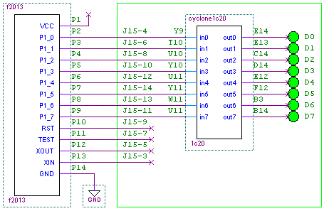
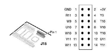
All of the microcontroller's pins (except VCC and GND) connect to the 1c20 board through J15, but in this design I'll only use 8 pins: P1.0 - P1.7. The FPGA will just be wires - it'll connect in0 to out0, in1 to out1, et al. The 8 outputs, out0 - out7, will drive the 8 individual LEDs on the 1c20 board. Then I'll write some code for the f2013 which will drive a recognizable pattern onto P1.0 - P1.7, which will make the 8 LEDs blink. Sounds easy! But... how do I configure the FPGA?

Install the Altera design software (Quartus)
A free version of Altera's main design tool, Quartus, is available. Go to http://www.altera.com and look for the "Quartus Web Edition Software". I hope the installation procedure is self-explanatory. If you run into trouble, let me know.

Create and configure a quartus project
This can be done via the GUI, but I think I'll play with the scripting flow. This is based on tcl, which seems to be the lingua franca of the EDA world. Altera provides a command-line tool which executes tcl files, and a set of commands which manage projects, set design properties, etc. I'll only scratch the surface here. Let's get started! I created a tcl script, call it tb_1.tcl:

# Step 1: Create a new project called tb_1
project_new tb_1
project_open tb_1

# Step 2: Project settings:
# a. Choose the type of FPGA
set_global_assignment -name FAMILY Cyclone
set_global_assignment -name DEVICE EP1C20F400C7
# b. Any pins which aren't otherwise defined should be inputs.
set_global_assignment -name RESERVE_ALL_UNUSED_PINS "AS INPUT TRI-STATED"
# c. Declare the top-level file (well, the only file):
set_global_assignment -name VERILOG_FILE top.v
set_global_assignment -name TOP_LEVEL_ENTITY top

# Step 3: Set pin assignments. This is where the top-level ports of the testbench
# design are mapped to actual physical FPGA pins.

set_location_assignment PIN_Y9 -to in[0]
set_location_assignment PIN_T10 -to in[1]
set_location_assignment PIN_V10 -to in[2]
set_location_assignment PIN_Y10 -to in[3]
set_location_assignment PIN_U11 -to in[4]
set_location_assignment PIN_Y11 -to in[5]
set_location_assignment PIN_W11 -to in[6]
set_location_assignment PIN_V11 -to in[7]
set_location_assignment PIN_E14 -to out[0]
set_location_assignment PIN_E13 -to out[1]
set_location_assignment PIN_C14 -to out[2]
set_location_assignment PIN_D14 -to out[3]
set_location_assignment PIN_E12 -to out[4]
set_location_assignment PIN_F12 -to out[5]
set_location_assignment PIN_B3 -to out[6]
set_location_assignment PIN_B14 -to out[7]

# Step 4. That's all!
project_close

To execute this tcl script, I go to an empty directory, open a bash shell (use Quartus' version, in <quartus>/bin/cygwin/bin/, if you don't already have one handy), and run

quartus_sh -t tb_1.tcl

Now the directory contains a few new things: files tb_1.qsf and tb_1.qpf, and a db directory. The qsf file seems to be nearly a copy of tb_1.tcl, with some extra stuff added. Comments in the qsf file advise me not to modify the file. Well, ok.

Specify the design's logic
In tb_1.tcl, I declared that the project's top-level entity would be "top", and that there would be a verilog file called "top.v". To deliver on my promise, I must create a verilog file called "top.v" which defines a module "top" containing all the ports that I made pin assignments for. Here's that verilog file:


module top(
  in,
  out
);

  input [7:0] in;
  output [7:0] out;

  assign out = in;

endmodule

Compile the design
Another tcl script, tb_1_compile.tcl:

# Compile the project:
# quartus_sh -t tb_1_compile.tcl
load_package flow
project_open tb_1
execute_flow -compile
project_close

Executing this tcl script takes 1 minute 22 seconds on my ancient laptop. The result is the FPGA configuration file, tb_1.sof.

Configure the FPGA
I've got a USB-Blaster for configuring my board. Here's the gratuitously-obscure command to configure the FPGA:


quartus_pgm --mode=jtag --cable=USB-Blaster --operation=p\;tb_1.sof

Results and wrapup
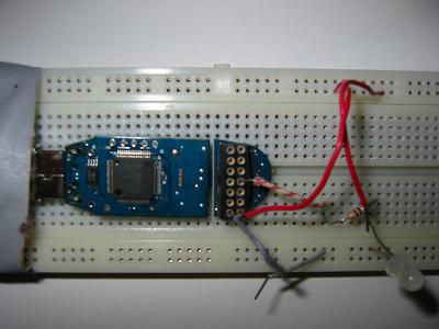
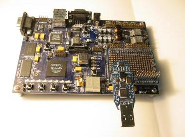
With the f2013 plugged into the santa cruz connector board plugged into the 1c20 board, a USB cable plugged into the f2013 (for power) and tb_1.sof downloaded into the FPGA, I actually do see blinking lights on the 8 LEDs! This is the result of whatever simple program I last programmed into the f2013. Next time I'll start fresh with a new f2013 software project, and blink some LEDs intentionally.

June 24, 2007

IAR IDE Flow

The ez430-f2013 comes with an IDE by IAR. It's a usable tool, but learning to use it isn't exactly straightforward - more a matter of trial and error. And, sadly, there doesn't seem to be a tutorial to introduce the basic concepts. So, here's a quick note on how to write some firmware for the f2013.


  1. Start the IDE, "IAR Embedded Workbench". Cancel the initial dialog "Embedded Workbench Startup" (if there were a "Create New Workspace" option here, I'd use it - but there isn't)

  2. Create a new workspace: File/New/Workspace

  3. Create and save a new project: Project/Create New Project...

    • Select tool chain MSP430 (the only option I see)

    • Select project template C/main

    • Save the project to some empty directory. I like a short but meaningful project name.


  4. Configure the new project: right-click on the project in the workspace window and select Options...

    • General Options/Target/Device: MSP430F2013

    • C/C++ Compiler/List/Output List File: check the checkbox (this is not essential, but I like having a list file)

    • Debugger/Setup/Driver: FET Debugger

    • FET Debugger/Setup/Connection: TI USB FET


  5. Write some code: main.c was created automatically, and is a compilable stub that does nothing. Fill in the stub with something interesting. If you like blinking LEDs, try this:

    #include "msp430x20x1.h"
    void main(void)
    {
      WDTCTL = WDTPW + WDTHOLD; // Stop watchdog timer
      P1DIR |= 0x01;

      for (;;)
      {
        volatile unsigned int i;

        P1OUT ^= 0x01;

        i = 10000;
        do i--;
        while (i != 0);
      }
    }


  6. Compile the code. Right-click on the project in the workspace window and select "Make". (The first time, you'll be prompted to save the new workspace. Funny timing, that. I've been using the same name for the workspace that I did for the project. I wonder if this is a good idea.)

  7. Download and debug the new application. In the Project menu, select Debug (or just type ^D). What happens? First the IDE writes the application into the f2013's flash. Then it starts debugging, stopping at the first code line. Select Debug/Go, or hit F5 to run the application. Notice that there's no "programming the device" step here - just debug the application, and as a side effect the device will be programmed. This seems a bit weird to me.

That's it! In the future I'll be exploring ways to run the tools from the command line, but at the moment using the GUI seems ok.

June 25, 2007

Ordinary Blinking Lights

I've given the f2013 8 bright shiny green LEDs to talk to; it's time to put those LEDs to work.

Edit: grr. The blog inserts bogus html directives into my pasted embedded youtube video reference, which confuses IE. For now, you'll have to click on a link to see the video.
Edit: no longer grr. I asked movabletype to not insert html tags for me.

There's a lot going on in this blurry video. On the lower left, the 8 green LEDs are throbbing nicely. On the lower right, you can see the LED on the f2013 board (P1.0) throbbing as well. The 7-segment digits display the number "02". Above them, another green LED blinks - that LED is just reporting that the 1c20 board configured itself from epcs flash. Lastly, above that, the power LED glows green.

PWM and ramp
I'm using PWM to brighten and dim the 8 LEDs. Each LED has a threshold value and a direction. A counter counts from 0 to a terminal count; each LED is off until its threshold value is reached, then on. After each count cycle, the threshold and direction values are updated. This is a purely software bit-twiddling operation, using none of the fabulous hardware features of the f2013. Here's my resource consumption report, excerpted from the list file:

148 bytes in segment CODE
4 bytes in segment DATA16_AN
24 bytes in segment DATA16_C

Updated testbench:
A note on this testbench: it's slightly improved from the previous one. As before, it connects its 8 inputs to the 8 LEDs; it also drives a version number ("02") onto the 2 seven-segment display digits on the 1c20 board. Going forward I'll give each new testbench its own ID, so I can verify at a glance that the testbench matches the f2013 firmware.

Manifest
For reference and archiving, here are all the source files.
main.c (obl firmware )
ordinary_blinking_lights.zip (archived workspace, project, source code)
top.v (top-level verilog file for testbench 02)
tb_2.zip (archived testbench 02 source files)

About June 2007

This page contains all entries posted to Aaron's Sandbox in June 2007. They are listed from oldest to newest.

July 2007 is the next archive.

Many more can be found on the main index page or by looking through the archives.

Powered by
Movable Type 3.31